Cvd Graphene Copper Etching

Clean And Efficient Transfer Of Cvd Grown Graphene By Electrochemical Etching Of Metal Substrate Sciencedirect

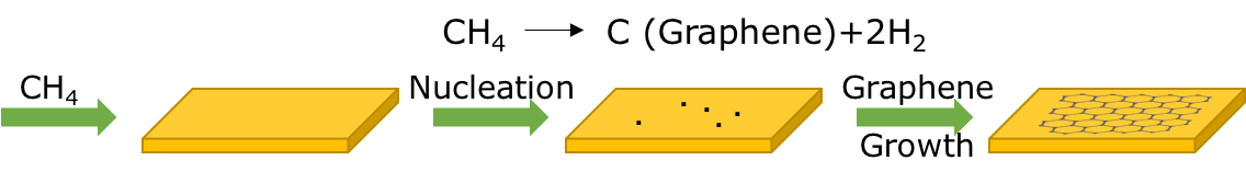
Cvd Graphene Growth Transfer Ishigami Group Wiki

New Way To Make Cheap Graphene Thermoelectric Materials Material Science Nanotechnology

Chemical Etching Of Copper Foils For Single Layer Graphene Growth By Chemical Vapor Deposition Sciencedirect

Schematic Illustration For The Preparation Of Cvd Graphene Strips Download Scientific Diagram
Cvd Graphene

After the copper was etched the pmma pva graphene block was rinsed with deionized water three times at 0 c and transferred onto a 100 nm thick sio 2 si substrate.
Cvd graphene copper etching.

Structure And Fabrication Process Of Cvd Grown Graphene On Pet Eva Download Scientific Diagram

Schematics Of The Transfer Process A Chemical Vapor Deposition Cvd Download Scientific Diagram

Monolayer Graphene Transfer Process To Polymeric Substrates A Download Scientific Diagram

Synthesis Based Application Of Graphene Nanotechnology Transistors Touch Screen
Source : pinterest.com
